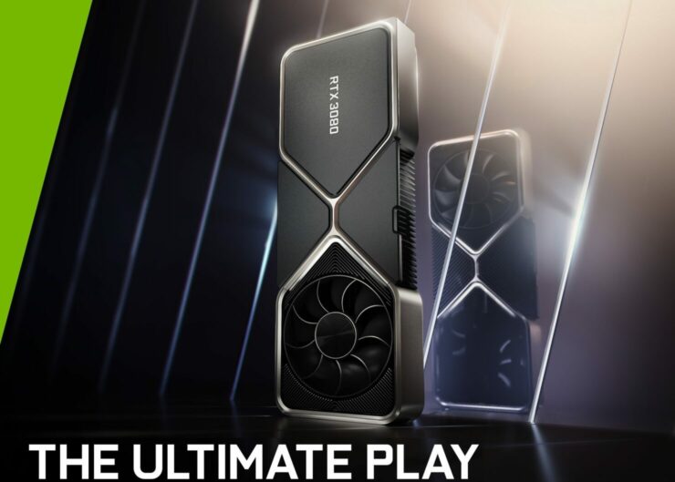
The NVIDIA GeForce RTX 3080 12 GB graphics card is indeed real and coming to the market soon with upgraded specifications as reported by Videocardz.
NVIDIA GeForce RTX 3080 12 GB To Please Miners More Than Gamers: Specs Leak Confirms 8960 Cores, 384-bit Bus & 20% Faster Mining Performance
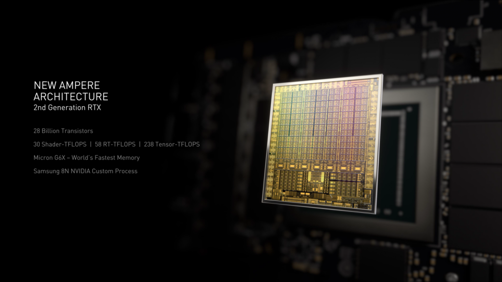
At the heart of the NVIDIA GeForce RTX 3080 12 GB graphics card lies the GA102 GPU. The GA102 is one of the many Ampere GPUs that we have seen in the high-end gaming segment and is so far the fastest gaming GPU that NVIDIA has produced. The GPU is based on Samsung’s 8nm custom process node designed specifically for NVIDIA and features a total of 28 Billion transistors. It measures at 628mm2 which makes it the 2nd biggest gaming GPU ever produced right below the Turing TU102 GPU.
For the GeForce RTX 3080 12 GB, NVIDIA has enabled a total of 70 SM units which results in a total of 8960 CUDA cores, a 3% increase over the standard RTX 3080. In addition to the CUDA cores, NVIDIA’s GeForce RTX 3080 also comes packed with next-generation RT (Ray-Tracing) cores, Tensor cores, and brand new SM or streaming multi-processor units. The card is suggested to have a TDP of 350W.
In terms of memory, the updated GeForce RTX 3080 comes packed with 12 GB of memory and that too is the next-generation GDDR6X design. With Micron’s latest and greatest graphics memory dies, the RTX 3080 can deliver GDDR6X memory speeds of 19.0 Gbps. That along with a bus interface of 384-bit will deliver a cumulative bandwidth of 912 GB/s or a 20% increase over the 10 GB variant.
NVIDIA GeForce RTX 30 ‘SUPER’ Series Graphics Card Specifications (Rumored):
| Graphics Card Name | NVIDIA GeForce RTX 3090 Ti | NVIDIA GeForce RTX 3090 | NVIDIA GeForce RTX 3080 Ti | NVIDIA GeForce RTX 3080 12 GB | NVIDIA GeForce RTX 3080 | NVIDIA GeForce RTX 3070 Ti 16 GB | NVIDIA GeForce RTX 3070 Ti | NVIDIA GeForce RTX 3070 | NVIDIA GeForce RTX 3060 Ti | NVIDIA GeForce RTX 3060 | NVIDIA GeForce RTX 3050 |
|---|---|---|---|---|---|---|---|---|---|---|---|
| GPU Name | Ampere GA102-350? | Ampere GA102-300 | Ampere GA102-225 | Ampere GA102-220? | Ampere GA102-200 | Ampere GA104-400 | Ampere GA104-400 | Ampere GA104-300 | Ampere GA104-200 | Ampere GA106-300 | Ampere GA106-150 |
| Process Node | Samsung 8nm | Samsung 8nm | Samsung 8nm | Samsung 8nm | Samsung 8nm | Samsung 8nm | Samsung 8nm | Samsung 8nm | Samsung 8nm | Samsung 8nm | Samsung 8nm |
| Die Size | 628.4mm2 | 628.4mm2 | 628.4mm2 | 628.4mm2 | 628.4mm2 | 395.2mm2 | 395.2mm2 | 395.2mm2 | 395.2mm2 | 276mm2 | 276mm2 |
| Transistors | 28 Billion | 28 Billion | 28 Billion | 28 Billion | 28 Billion | 17.4 Billion | 17.4 Billion | 17.4 Billion | 17.4 Billion | 13.2 Billion | 13.2 Billion |
| CUDA Cores | 10752 | 10496 | 10240 | 8960 | 8704 | 6144 | 6144 | 5888 | 4864 | 3584 | 3072? |
| TMUs / ROPs | 336 / 112 | 328 / 112 | 320 / 112 | 280 / 104 | 272 / 96 | 184 / 96 | 184 / 96 | 184 / 96 | 152 / 80 | 112 / 64 | TBC |
| Tensor / RT Cores | 336 / 84 | 328 / 82 | 320 / 80 | 280 / 70 | 272 / 68 | 184 / 46 | 184 / 46 | 184 / 46 | 152 / 38 | 112 / 28 | TBC |
| Base Clock | TBA | 1400 MHz | 1365 MHz | TBA | 1440 MHz | TBA | 1575 MHz | 1500 MHz | 1410 MHz | 1320 MHz | TBC |
| Boost Clock | TBA | 1700 MHz | 1665 MHz | TBA | 1710 MHz | TBA | 1770 MHz | 1730 MHz | 1665 MHz | 1780 MHz | TBC |
| FP32 Compute | TBA | 36 TFLOPs | 34 TFLOPs | TBA | 30 TFLOPs | TBA | 22 TFLOPs | 20 TFLOPs | 16 TFLOPs | 13 TFLOPs | TBC |
| RT TFLOPs | TBA | 69 TFLOPs | 67 TFLOPs | TBA | 58 TFLOPs | TBA | 44 TFLOPs | 40 TFLOPs | 32 TFLOPs | 25 TFLOPs | TBC |
| Tensor-TOPs | TBA | 285 TOPs | 273 TOPs | TBA | 238 TOPs | TBA | 183 TOPs | 163 TOPs | 192 TOPs | 101 TOPs | TBC |
| Memory Capacity | 24 GB GDDR6X | 24 GB GDDR6X | 12 GB GDDR6X | 12 GB GDDR6X | 10 GB GDDR6X | 16 GB GDDR6X | 8 GB GDDR6X | 8 GB GDDR6 | 8 GB GDDR6 | 12 GB GDDR6 | 8 GB GDDR6 |
| Memory Bus | 384-bit | 384-bit | 384-bit | 384-bit | 320-bit | 256-bit | 256-bit | 256-bit | 256-bit | 192-bit | 128-bit |
| Memory Speed | 21 Gbps | 19.5 Gbps | 19 Gbps | 19 Gbps | 19 Gbps | 21 Gbps | 19 Gbps | 14 Gbps | 14 Gbps | 16 Gbps | TBC |
| Bandwidth | 1008 GB/s | 936 GB/s | 912 Gbps | 912 Gbps | 760 GB/s | 672 GB/s | 608 GB/s | 448 GB/s | 448 GB/s | 384 GB/s | TBC |
| TGP | 450W | 350W | 350W | 350W | 320W | ~300W | 290W | 220W | 175W | 170W | 150W? |
| Price (MSRP / FE) | $1499 US | $1499 US | $1199 | $999 US? | $699 US | $599 US? | $599 US | $499 US | $399 US | $329 US | $279 US? |
| Launch (Availability) | 27th January 2022 | 24th September 2020 | 3rd June 2021 | Q1 2022? | 17th September 2020 | Q1 2022? | 10th June, 2021 | 29th October 2020 | 2nd December 2020 | 25th February 2021 | 27th January 2022 |
As for the card itself, it is stated to launch in late January as suggested in a rumor from yesterday which mentioned that this card and the GeForce RTX 3070 Ti 16 GB have been delayed by NVIDIA and the only card to make it on time for launch on 27th January would be the GeForce RTX 3090 Ti. In terms of performance, the graphics card is expected to be just slightly faster in gaming with a 5 percent average boost but for miners, the card might hold a special spot as the updated memory will help it push crypto performance by up to 20% over the 10 GB variant. The card is stated to get 52 MH/s over the 43 MH/s that the LHR variant of the RTX 3080 produces. With that said, there are currently several LHR hacks and unlocks out in the market that can push the performance further up.
This would mean that the RTX 3080 12 GB is likely another card that would be going in the hands of miners first than gamers. The pricing is expected to be close to $999 US MSRP but we know that the actual price is going to be way higher than what MSRP’s are these days. The NVIDIA GeForce RTX 3080 12 GB would also tackle Intel’s high-end ARC lineup though that is only expected to be as fast as the RTX 3070 Ti.
The post NVIDIA GeForce RTX 3080 12 GB Graphics Card Specs Leak Out – 8960 Cores, 384-bit Bus & 20% Faster Than 3080 In Mining by Hassan Mujtaba appeared first on Wccftech.
