During the 67th International Electron Devices Meeting, held this year in San Francisco, CA, Samsung and IBM announced during their discussion on “3D at the Device Level”, revealing that the two tech companies had collaborated to achieve a major breakthrough in design techniques for next-gen semiconductor chips. This new technology allows for transistors to be stacked vertically, essentially adding improved efficiency in power or higher levels of performance.
Samsung and IBM reveal breakthrough VTFET semiconductor technology, offering higher levels of productivity and efficiency
During the talk, the two companies explained how, by redirecting the flow of the current from horizontally to vertically, they could not only reduce the size of the semiconductor chips, but also make them more powerful and efficient.
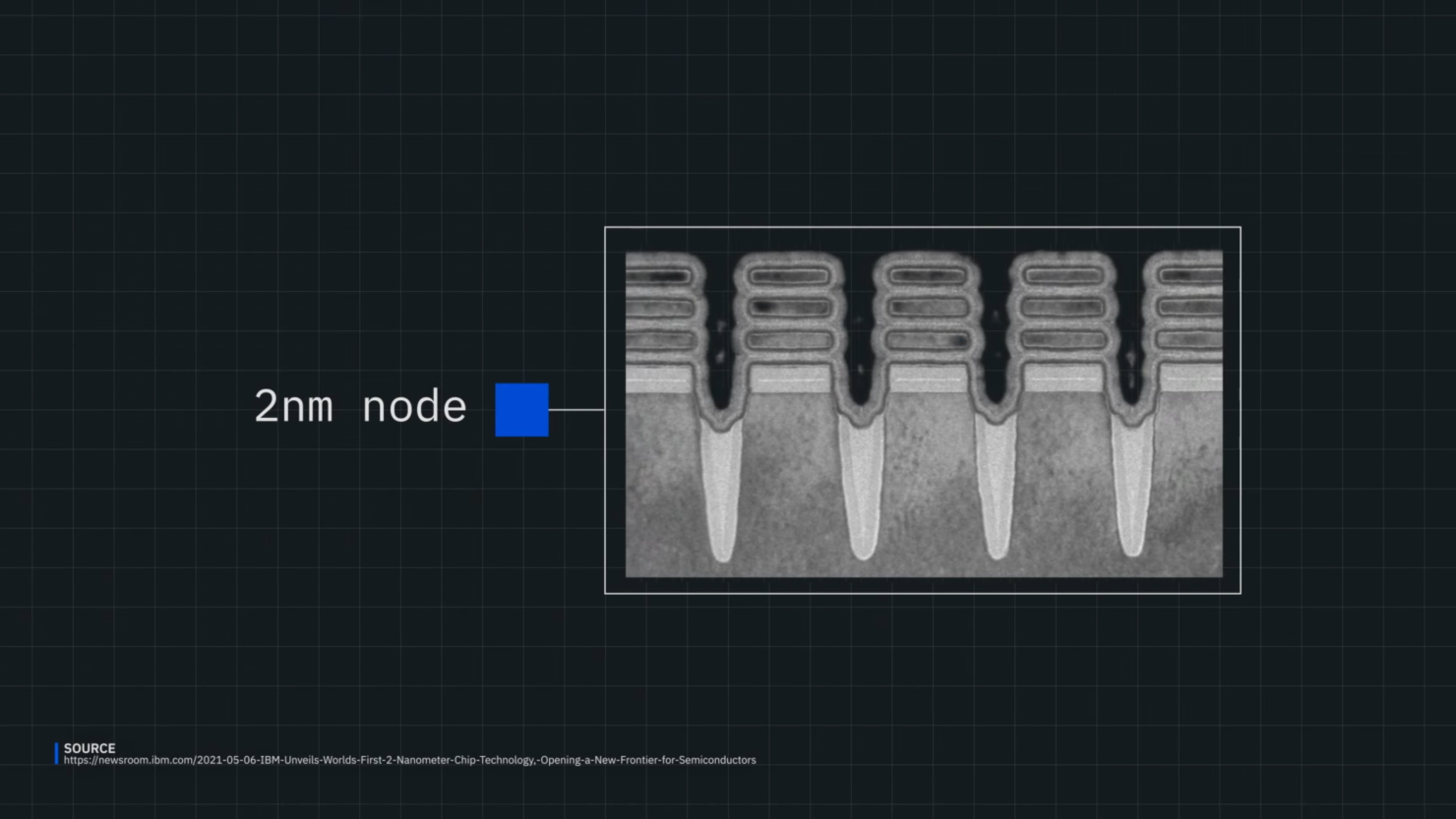
CMOS transistors are built in a lateral, or horizontal, fashion, and countless advances over decades have shrunk their dimensions so that billions of them can now be put on a chip, in accordance with the predictions of Moore’s Law. But shrinking transistors further in order to boost chip performance and add new features is difficult and costly. Would orienting them vertically instead of horizontally save space and make it easier to extend the life of Moore’s Law? Inspired by trench-based DRAM vertical access transistors, a team from IBM and Samsung will describe how they turned transistor architecture on its side, with CMOS devices built using so-called Vertical-Transport Nanosheets (VTFETs) on bulk silicon and with a 45nm gate pitch.
— Paper #26.1, “Vertical-Transport Nanosheet Technology for CMOS Scaling beyond Lateral-Transport Devices,” H. Jagannathan et al, IBM/Samsung
Previously, semiconductor chips would be placed flat upon the surface of the silicon while the current would flow horizontally. This new design allows the transistors to sit perpendicular, instead of parallel to the surface of the semiconductor chip. The new technology will allow manufacturing companies to bypass the limiting performances of Moore’s Law, allowing for energy to be salvaged due to the low consumption of power.
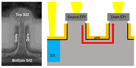
Cross-sectional TEM of a VTFET nanosheet transistor (the source can be located at either the top or bottom for design flexibility) and next to it is a schematic of an I/O device FET co-integrated with the VTFET. Source: IEDM Paper 26.1, “3D at the Device Level”
Samsung and IBM’s effort for vertically stacking transistors for more efficiency and performance is called Vertical Transport Field Effect Transistors, or VTFET. The collaboration between the two companies is expected to offer twice the performance, or up to 85% improved efficiency of power, compared to the current FinFET structure design. Cryptocurrency miners will see improvements in power efficiency, and the impact of the environment will essentially see an improvement as well.
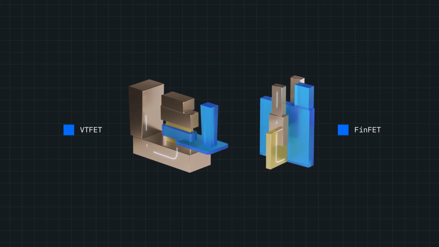
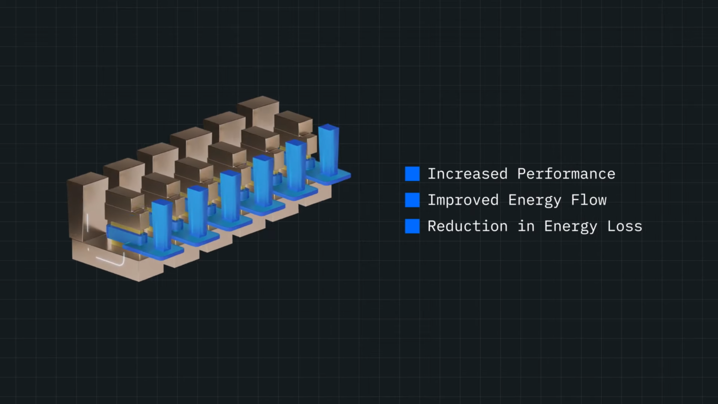

The vertical devices offer the opportunity for continued scaling because gate length and spacer size – two key elements which determine gate pitch (the distance between transistors) – can be optimized in ways that aren’t possible horizontally. Also, the VTFET devices promise to deliver outstanding operating voltage and drive current as a result of reduced electrostatic and parasitic losses (SS=69/68 mV/dec and DIBL= <30mV). To validate the concept, the researchers used the VTFETs to make functional ring oscillators (test circuits), which demonstrated ~50% reduction in capacitance vs. a lateral design reference.
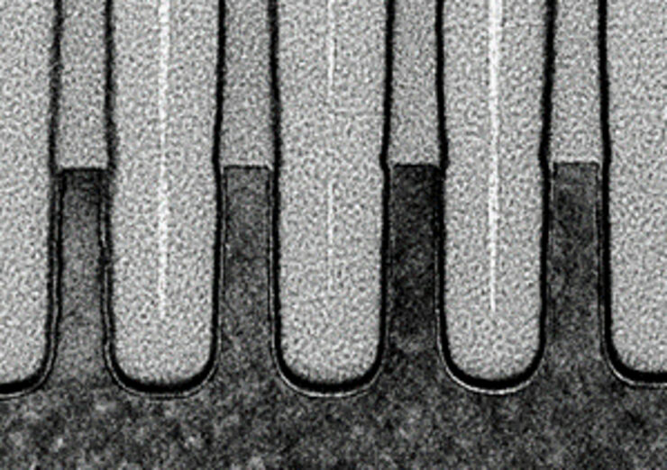
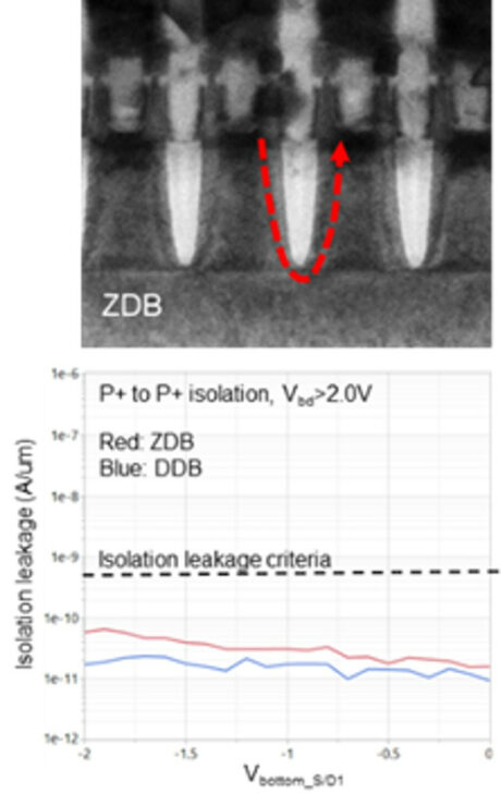 A TEM of the zero diffusion break formation structure, showing that it meets isolation criteria at high circuit densities. Source: IEDM Paper 26.1 “3D at the Device Level”
No word yet on when the new VTFET technology will be seen on a commercial product level. Intel, as well as other tech giants, are noted as creating new angstrom-scale chips, with Intel estimating a release date sometime during the last quarter of 2024 under the branding of Intel 20A.
Source: IEDM
The post Samsung joins forces with IBM to advance breakthroughs in semiconductor chip design by Jason R. Wilson appeared first on Wccftech.