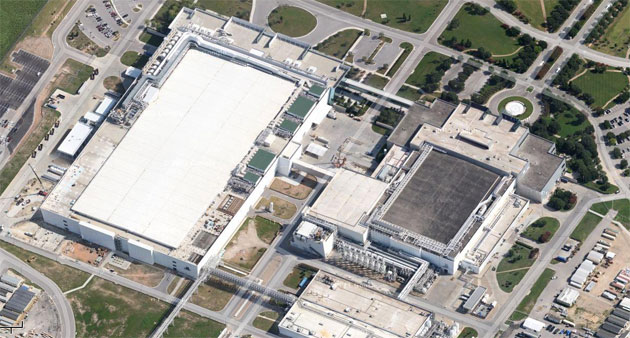
Korean chaebol Samsung Group’s chipmaking division Samsung Foundry is set to announce its plans to build a $17 billion chip plant in the United States this week. Samsung’s vice chairman, Mr. Lee-jae Yong visited the U.S. over the weekend where he met with government officials and heads of technology and biopharmaceutical firms in his first high profile visit since being released from jail for bribery charges. The chip manufacturing facility will be the second of its kind being recently built in the U.S., with another one belonging to the Taiwan Semiconductor Manufacturing Company (TSMC) already under construction in Arizona.
Samsung Chief Visits U.S. To Discuss Chip Plant, Meets With Microsoft and Amazon Representatives
News of Mr. Lee’s trip to the U.S. broke last week when South Korean industry sources speculated that the executive would make the journey to finalize the location for Samsung’s new chip manufacturing facility in the country. The Korean company is currently evaluating several sites for the plant, and it appears that a decision is near since it has withdrawn some documents submitted to authorities in Texas. The state is one of three potential locations, with the other two being in Arizona and New York.
Now, according to several Korean publications, not only has Mr. Lee made the trip but that Samsung will announce the decision for the $17 billion facility later this week. Specifically, Business Korea quotes a U.S. congressman as providing the timeline for the announcement.
According to the publication:
A U.S. Congressional official who met with Lee said Samsung Electronics would officially announce its plan to build US$1.7 billion foundry in the United States this week.
The “$1.7 billion” outlined above appears to be a typographical error as several publications such as Reuters have placed a $17 billion price tag for the American chip plant.
In addition to Business Korea, Donga also quotes a Congress official highlighting that the decision to announce the plant has been made.
Donga reports that:
On November 18, Lee met with members of the U.S. Congress responsible for laws on supporting semiconductor investment to request support to pass related laws. An official who attended the meeting said that candidate sites for the foundry will be trimmed down and officially announced this week.
After his meetings in Washington, Mr. Lee traveled to the West Coast to meet with Microsoft Corporation’s chief executive officer Mr. Satya Nadella and representatives from Amazon. He discussed emerging technologies such as augmented and virtual realities and semiconductors with the Microsoft chief.
During the trip, Mr. Lee also met with executives of vaccine manufacturer Moderna and wireless network operator Verizon. Samsung has been manufacturing Moderna’s vaccine for the ongoing pandemic and the pair discussed methods to extend their cooperation at this and other fronts.
Samsung’s $17 billion U.S. chip fab will be the company’s second such facility in the U.S. It is expected to commence production from 2024, and churn out semiconductors manufactured using advanced manufacturing processes.
The Korean company plans to make the first deliveries of its 3-nanometer chips next year, as it races to catch up with TSMC who is the world’s largest contract chip manufacturer. These will utilize a new transistor design called Gate-All-Around or GAAFET for short. TSMC, on the other hand, will rely on traditional FinFET transistors for its 3nm process.
Efforts to boost North American semiconductor fabrication come as the world reels from a historic chip shortage that has affected the personal computing, communications and automotive sectors. Industry executives expect that the shortage will last throughout 2023, while some analysts worry that an overabundance of silicon might harm companies such as TSMC who can end up dealing with reduced orders.
The post Samsung To Announce $17 Billion Chip Plant This Week After Executive’s Visit by Ramish Zafar appeared first on Wccftech.