Rumored specifications of the next-generation AMD RDNA 3 powered Radeon RX 7900 XT & NVIDIA Ada Lovelace powered GeForce RTX 4090 graphics cards have been detailed once again. The rumors come from Greymon55 who has been actively posting details regarding upcoming hardware such as CPUs and GPUs over on his Twitter feed for a while now.
AMD RDNA 3 & NVIDIA Ada Lovelace GPU Powered Next-Gen Flagship Radeon RX 7900 XT & GeForce RTX 4090 Graphics Cards Detailed
The AMD RDNA 3 powered Navi 31 and Ada Lovelace-powered AD102 GPUs are expected to bring huge performance improvements and will also be the most power-hungry chips ever made. While NVIDIA is aiming for a monolithic approach with its Ada Lovelace architecture, AMD will utilize a full MCM design which it has already taken leadership in with the launch of the CDNA 2 powered MI200 series ‘Aldebaran’. AMD will leverage the same MCM technology for consumer-end & gaming GPUs now. So let’s talk about the latest rumored specifications that we have got from the leaker:
AD102
5nm TSMC
144SM 18432CUDA
384bit 24G GDDR6X 21Gbps?
2.3~2.5GHz?
85~92T FP32?— Greymon55 (@greymon55) November 9, 2021
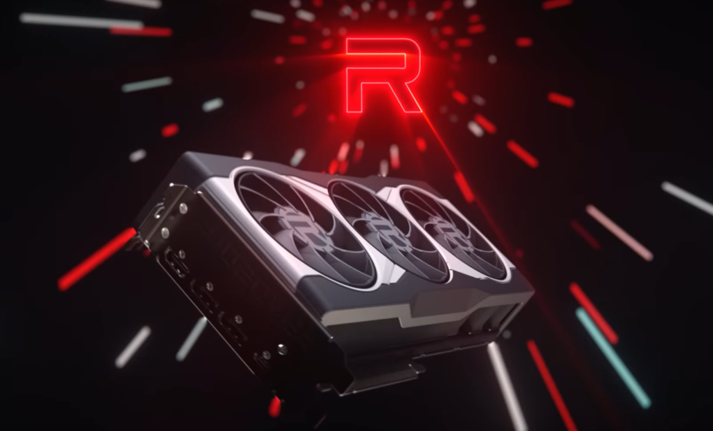
AMD Radeon RX 7900 XT Graphics Card – RDNA 3 Powered Navi 31 Flagship GPU
The AMD Navi 31 GPU, the flagship RDNA 3 chip, would power the next-gen Radeon RX 7900 XT graphics card. We have heard that AMD will drop CU (Compute Units) in favor of WGP (Work Group Processors) on its next-gen RDNA 3 GPUs. Since Navi 31 is an MCM GPU, it will feature two key IPs, a GCD (Graphics Core Die) based on TSMC’s 5nm process and an MCD (Multi-Cache Die) based on the TSMC 6nm process node. Earlier rumors suggest that AMD has already tapped out its Navi 31 GPU die.
The Navi 31 GPU configuration shown here features two GCD’s (Graphics Core Die) and a single MCD (Multi-Cache Die). Each GCD has 3 Shader Engines (6 in total) and each Shader Engine has 2 Shader Arrays (2 per SE / 6 per GCD / 12 in total). Each Shader Array is composed of 5 WGPs (10 per SE / 30 per GCD / 60 in total) and each WGP features 8 SIMD32 units with 32 ALUs (40 SIMD32 per SA / 80 per SE / 240 per GCD / 480 in total). These SIMD32 units combine to make up 7,680 cores per GCD and 15,360 cores in total.

Performance-wise, the GPU is expected to feature a clock speed of 2.4 – 2.5 GHz which puts its theoretical performance at around 75 TFLOPs (FP32). This is an insane 226% improvement vs a Radeon RX 6900 XT graphics card.
The Navi 31 (RDNA 3) MCD will be linked to the dual GCD’s via a next-generation Infinity Fabric interconnect and feature 256-512 MB of Infinity Cache. Each GPU should also feature 4 memory connect links (32-bit). That’s a total of 8 32-bit memory controllers for a 256-bit bus interface. It is stated that the card will feature up to 32 GB of GDDR6 memory running at 18 Gbps pin speeds & that delivers up to 576 GB/s bandwidth. Another rumor that appeared recently suggests that AMD will be using 3D Infinity Cache technology on its RDNA 3 lineup which will integrate the new cache in vertical stacks on the GPUs, similar to how the Vermeer-X chips will stack L3 cache over the CCD.
AMD RDNA GPU (Generational Comparison) Preliminary:
| GPU Name | Navi 10 | Navi 21 | Navi 31 |
|---|---|---|---|
| GPU Process | 7nm | 7nm | 5nm (6nm?) |
| GPU Package | Monolithic | Monolithic | MCD (Multi-Chiplet Die) |
| Shader Engines | 2 | 4 | 6 |
| GPU WGPs | 20 | 40 | 30 (Per MCD) 60 (In Total) |
| SPs Per WGP | 128 | 128 | 256 |
| Compute Units (Per Die) | 40 | 80 | 120 (per MCD) 240 (in total) |
| Cores (Per Die) | 2560 | 5120 | 7680 |
| Cores (Total) | 2560 | 5120 | 15360 (2 x MCD) |
| Memory Bus | 256-bit | 256-bit | 256-bit |
| Memory Type | GDDR6 | GDDR6 | GDDR6 |
| Memory Capacity | 8 GB | 16 GB | 32 GB |
| Infinity Cache | N/A | 128 MB | 256-512 MB |
| Flagship SKU | Radeon RX 5700 XT | Radeon RX 6900 XTX | Radeon RX 7900 XT |
| TBP | 225W | 330W | 350-550W |
| Launch | Q3 2019 | Q4 2020 | Q4 2022 |
NVIDIA GeForce RTX 4090 Graphics Card – Ada Lovelace Powered AD102 Flagship GPU
Based upon previous rumors, there have been whispers that NVIDIA would utilize TSMC’s N5 (5nm) process node for its Ada Lovelace GPUs. This includes the AD102 SKU too which will be an entirely monolithic design. In his latest tweet which talks about the specific GPU configurations, the AD102 GPU is said to feature a clock speed as high as 2.5 GHz (2.3 GHz average boost). The specific tweet states that the GPU clock for Ada Lovelace ‘AD102’ could be 2.3 GHz or greater so let’s take that as a baseline and previously leaked specifications to figure out where the performance should land.
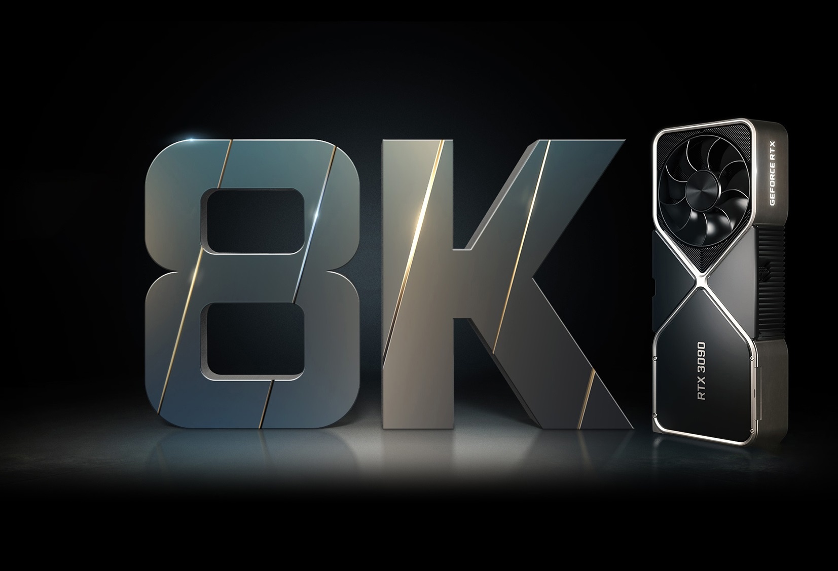
The NVIDIA AD102 “ADA GPU” appears to have 18432 CUDA Cores based on the preliminary specs (which can change), housed within 144 SM units. This is almost twice the cores present in Ampere which was already a massive step up from Turing. A 2.3-2.5 GHz clock speed would give us up to 85 to 92 TFLOPs of compute performance (FP32). This is more than twice the FP32 performance of the existing RTX 3090 which packs 36 TFLOPs of FP32 compute power.
The 150% performance jump looks huge but one should remember that NVIDIA already gave a big jump in FP32 numbers this generation with Ampere. The Ampere GA102 GPU (RTX 3090) offers 36 TFLOPs while the Turing TU102 GPU (RTX 2080 Ti) offered 13 TFLOPs. That’s over a 150% increase in FP32 Flops but the real-world gaming performance increase for the RTX 3090 averaged at around 50-60% faster over the RTX 2080 Ti. So one thing we shouldn’t forget is that Flops don’t equal GPU gaming performance these days. Furthermore, we don’t know if 2.3-2.5 GHz is the average boost or the peak boost with the former meaning that there could be even higher compute potential for AD102.
Aside from that, the leaker also states that the NVIDIA GeForce RTX 40 flagship would retain a 384-bit bus interface, similar to the RTX 3090. What’s interesting is though that the leaker mentions G6X which means that NVIDIA won’t be moving to a new memory standard until after Ada Lovelace and utilize the higher pin-speeds of G6X of 21 Gbps for its next-generation cards before we see a newer standard (e.g. GDDR7). The card will feature 24 GB of memory so we can either expect single-sided 16Gb DRAM or dual-sided 8Gb DRAM modules.
NVIDIA CUDA GPU (RUMORED) Preliminary:
| GPU | TU102 | GA102 | AD102 |
|---|---|---|---|
| Architecture | Turing | Ampere | Ada Lovelace |
| Process | TSMC 12nm NFF | Samsung 8nm | 5nm |
| Graphics Processing Clusters (GPC) | 6 | 7 | 12 |
| Texture Processing Clusters (TPC) | 36 | 42 | 72 |
| Streaming Multiprocessors (SM) | 72 | 84 | 144 |
| CUDA Cores | 4608 | 10752 | 18432 |
| Theoretical TFLOPs | 16.1 | 37.6 | ~90 TFLOPs? |
| Memory Type | GDDR6 | GDDR6X | GDDR6X |
| Memory Bus | 384-bit | 384-bit | 384-bit |
| Memory Capacity | 11 GB (2080 Ti) | 24 GB (3090) | 24 GB (4090?) |
| Flagship SKU | RTX 2080 Ti | RTX 3090 | RTX 4090? |
| TGP | 250W | 350W | 450-650W? |
| Release | Sep. 2018 | Sept. 20 | 2022 (TBC) |
The NVIDIA Ada Lovelace GPUs will power the next-generation GeForce RTX 40 graphics cards that will go head-on with AMD’s RDNA 3 based Radeon RX 7000 series graphics cards. There’s still some speculation regarding the use of MCM by NVIDIA. The Hopper GPU, which is primarily aimed at the Datacenter & AI segment, is allegedly taping out soon and will feature an MCM architecture. NVIDIA won’t be using an MCM design on its Ada Lovelace GPUs so they will keep the traditional monolithic design.
Which next-generation GPUs are you looking forward to the most?
- AMD RDNA 3 (Navi 3X Radeon RX GPUs)
- NVIDIA Ada Lovelace (GeForce RTX GPUs)
- Intel ARC Alchemist (ARC Graphics Cards)
View ResultsPoll Options are limited because JavaScript is disabled in your browser.
The post AMD & NVIDIA Next-Gen Flagship GPUs Detailed: RDNA 3 Radeon RX 7900 XT With 15360 Cores, Ada Lovelace GeForce RTX 4090 With 18432 Cores by Hassan Mujtaba appeared first on Wccftech.