A mysterious NVIDIA GPU known as GPU-N which could possibly be the first look at the next-gen Hopper GH100 chip has been revealed in a new research paper published by the green team (as discovered by Twitter user, Redfire).
NVIDIA Research Paper Talks ‘GPU-N’ With MCM Design & 8576 Cores, Could This Be Next-Gen Hopper GH100?
The research paper ‘GPU Domain Specialization via Composable On-Package Architecture’ talks about a next-generation GPU design as the most practical solution for maximizing low-precision matrix math throughput to boost Deep Learning performance. The ‘GPU-N’ and its respective COPA designs have been discussed along with their possible specifications and simulated performance results.
The ‘GPU-N’ is said to feature 134 SM units (vs 104 SM units of A100). This makes up a total of 8576 cores or a 24% increase over the current Ampere A100 solution. The chip has been measured at 1.4 GHz, the same theoretical clock speed of the Ampere A100 and Volta V100 (not to be confused as the final clocks). Other specifications include a 60 MB L2 cache, a 50% increase over Ampere A100, and a DRAM bandwidth of 2.68 TB/s that can scale up to 6.3 TB/s. The HBM2e DRAM capacity is 100 GB and can be expanded up to 233 GB with the COPA implementations. It is configured around a 6144-bit bus interface at clock speeds of 3.5 Gbps.
| Configuration | NVIDIA V100 | NVIDIA A100 | GPU-N |
|---|---|---|---|
| SMs | 80 | 108 | 134 |
| GPU frequency (GHz) | 1.4 | 1.4 | 1.4 |
| FP32 (TFLOPS) | 15.7 | 19.5 | 24.2 |
| FP16 (TFLOPS) | 125 | 312 | 779 |
| L2 cache (MB) | 6 | 40 | 60 |
| DRAM BW (GB/s) | 900 | 1,555 | 2,687 |
| DRAM Capacity (GB) | 16 | 40 | 100 |
Coming to the performance numbers, the ‘GPU-N’ (presumably Hopper GH100) produces 24.2 TFLOPs of FP32 (24% increase over A100) and 779 TFLOPs FP16 (2.5x increase over A100) which sounds really close to the 3x gains that were rumored for GH100 over A100. Compared to AMD’s CDNA 2 ‘Aldebaran’ GPU on the Instinct MI250X accelerator, the FP32 performance is less than half (95.7 TFLOPs vs 24.2 TFLOPs) but the FP16 performance is 2.15x higher.
From previous information, we know that NVIDIA’s H100 accelerator would be based on an MCM solution and utilize TSMC’s 5nm process node. Hopper is supposed to have two next-gen GPU modules so we are looking at 288 SM units in total. We can’t give a rundown on the core count yet since we don’t know the number of cores featured in each SMs but if it’s going to stick to 64 cores per SM, then we get 18,432 cores which are 2.25x more than the full GA100 GPU configuration. NVIDIA could also leverage more FP64, FP16 & Tensor cores within its Hopper GPU which would drive up performance immensely. And that’s going to be a necessity to rival Intel’s Ponte Vecchio which is expected to feature 1:1 FP64.
It is likely that the final configuration will come with 134 of the 144 SM units enabled on each GPU module and as such, we are likely looking at a single GH100 die in action. But it is unlikely that NVIDIA would reach the same FP32 or FP64 Flops as MI200’s without using GPU Sparsity.
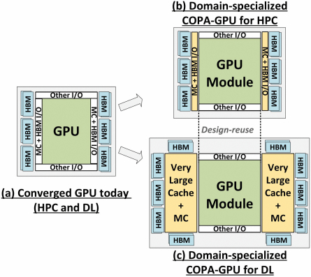
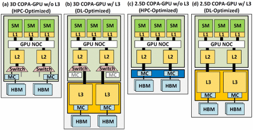
But NVIDIA may likely have a secret weapon in their sleeves and that would be the COPA-based GPU implementation of Hopper. NVIDIA talks about two Domain-Specialized COPA-GPUs based on next-generation architecture, one for HPC and one for DL segment. The HPC variant features a very standard approach which consists of an MCM GPU design and the respective HBM/MC+HBM (IO) chiplets but the DL variant is where things start to get interesting. The DL variant houses a huge cache on an entirely separate die that is interconnected with the GPU modules.
| Architecture | LLC Capacity | DRAM BW | DRAM Capacity |
|---|---|---|---|
| Configuration | (MB) | (TB/s) | (GB) |
| GPU-N | 60 | 2.7 | 100 |
| COPA-GPU-1 | 960 | 2.7 | 100 |
| COPA-GPU-2 | 960 | 4.5 | 167 |
| COPA-GPU-3 | 1,920 | 2.7 | 100 |
| COPA-GPU-4 | 1,920 | 4.5 | 167 |
| COPA-GPU-5 | 1,920 | 6.3 | 233 |
| Perfect L2 | infinite | infinite | infinite |
Various variants have been outlined with up to 960 / 1920 GB of LLC (Last-Level-Cache), HBM2e DRAM capacities of up to 233 GB, and bandwidth of up to 6.3 TB/s. These are all theoretical but given that NVIDIA has discussed them now, we may likely see a Hopper variant with such a design during the full unveil at GTC 2022.
NVIDIA Hopper GH100 ‘Preliminary Specs’:
| NVIDIA Tesla Graphics Card | Tesla K40 (PCI-Express) |
Tesla M40 (PCI-Express) |
Tesla P100 (PCI-Express) |
Tesla P100 (SXM2) | Tesla V100 (SXM2) | NVIDIA A100 (SXM4) | NVIDIA H100 (SMX4?) |
|---|---|---|---|---|---|---|---|
| GPU | GK110 (Kepler) | GM200 (Maxwell) | GP100 (Pascal) | GP100 (Pascal) | GV100 (Volta) | GA100 (Ampere) | GH100 (Hopper) |
| Process Node | 28nm | 28nm | 16nm | 16nm | 12nm | 7nm | 5nm |
| Transistors | 7.1 Billion | 8 Billion | 15.3 Billion | 15.3 Billion | 21.1 Billion | 54.2 Billion | TBD |
| GPU Die Size | 551 mm2 | 601 mm2 | 610 mm2 | 610 mm2 | 815mm2 | 826mm2 | TBD |
| SMs | 15 | 24 | 56 | 56 | 80 | 108 | 134 (Per Module) |
| TPCs | 15 | 24 | 28 | 28 | 40 | 54 | TBD |
| FP32 CUDA Cores Per SM | 192 | 128 | 64 | 64 | 64 | 64 | 64? |
| FP64 CUDA Cores / SM | 64 | 4 | 32 | 32 | 32 | 32 | 32? |
| FP32 CUDA Cores | 2880 | 3072 | 3584 | 3584 | 5120 | 6912 | 8576 (Per Module) 17152 (Complete) |
| FP64 CUDA Cores | 960 | 96 | 1792 | 1792 | 2560 | 3456 | 4288 (Per Module)? 8576 (Complete)? |
| Tensor Cores | N/A | N/A | N/A | N/A | 640 | 432 | TBD |
| Texture Units | 240 | 192 | 224 | 224 | 320 | 432 | TBD |
| Boost Clock | 875 MHz | 1114 MHz | 1329MHz | 1480 MHz | 1530 MHz | 1410 MHz | ~1400 MHz |
| TOPs (DNN/AI) | N/A | N/A | N/A | N/A | 125 TOPs | 1248 TOPs 2496 TOPs with Sparsity |
TBD |
| FP16 Compute | N/A | N/A | 18.7 TFLOPs | 21.2 TFLOPs | 30.4 TFLOPs | 312 TFLOPs 624 TFLOPs with Sparsity |
779 TFLOPs (Per Module)? 1558 TFLOPs with Sparsity (Per Module)? |
| FP32 Compute | 5.04 TFLOPs | 6.8 TFLOPs | 10.0 TFLOPs | 10.6 TFLOPs | 15.7 TFLOPs | 19.4 TFLOPs 156 TFLOPs With Sparsity |
24.2 TFLOPs (Per Module)? 193.6 TFLOPs With Sparsity? |
| FP64 Compute | 1.68 TFLOPs | 0.2 TFLOPs | 4.7 TFLOPs | 5.30 TFLOPs | 7.80 TFLOPs | 19.5 TFLOPs (9.7 TFLOPs standard) |
24.2 TFLOPs (Per Module)? (12.1 TFLOPs standard)? |
| Memory Interface | 384-bit GDDR5 | 384-bit GDDR5 | 4096-bit HBM2 | 4096-bit HBM2 | 4096-bit HBM2 | 6144-bit HBM2e | 6144-bit HBM2e |
| Memory Size | 12 GB GDDR5 @ 288 GB/s | 24 GB GDDR5 @ 288 GB/s | 16 GB HBM2 @ 732 GB/s 12 GB HBM2 @ 549 GB/s |
16 GB HBM2 @ 732 GB/s | 16 GB HBM2 @ 900 GB/s | Up To 40 GB HBM2 @ 1.6 TB/s Up To 80 GB HBM2 @ 1.6 TB/s |
Up To 100 GB HBM2e @ 3.5 Gbps |
| L2 Cache Size | 1536 KB | 3072 KB | 4096 KB | 4096 KB | 6144 KB | 40960 KB | 81920 KB |
| TDP | 235W | 250W | 250W | 300W | 300W | 400W | ~450-500W |
The post Mysterious NVIDIA ‘GPU-N’ Could Be Next-Gen Hopper GH100 In Disguise With 134 SMs, 8576 Cores & 2.68 TB/s Bandwidth, Simulated Performance Benchmarks Shown by Hassan Mujtaba appeared first on Wccftech.